
Fail:Wafer flats convention v2.svg

Algfail (SVG-fail, algsuurus 150 × 150 pikslit, faili suurus: 13 KB)
| See fail ja sellest kastist allapoole jääv kirjeldus pärinevad kesksest failivaramust Wikimedia Commons. | Faili lehekülg Commonsis |
Lühikirjeldus
| Kirjeldus |
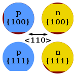
Wafer flats convention, based on Image:Wafer flats convention.PNG Conventional meaning of flats in semiconductor wafers. Red denotes material that has been removed. Wafer orientation is the orientation of the crystallographic plane in which the crystal grew. Wafer type indicated the type of doping.
|
| Kuupäev | |
| Allikas |
self-made, See vektorkujutis on valmistatud rakendusega Inkscape . |
| Autor | Twisp |
| Teised versioonid | Wafer flats convention.PNG |
Litsents
| Selle teose autoriõiguste valdajana annan selle teose avalikku omandisse. See kehtib üleilmselt. Kui see pole mõnes riigis õiguslikult võimalik: Annan kõigile õiguse seda teost kasutada ükskõik mille jaoks, ilma ühegi tingimuseta, kui seadus neid just ei sea. |
Faili ajalugu
Klõpsa kuupäeva ja kellaaega, et näha sel ajahetkel kasutusel olnud failiversiooni.
| Kuupäev/kellaaeg | Pisipilt | Mõõtmed | Kasutaja | Kommentaar | |
|---|---|---|---|---|---|
| viimane | 25. september 2013, kell 00:40 | | 150 × 150 (13 KB) | Cepheiden | fixed position of secondary flat Silicon processing for the VLSI era - Vol. 1 - Process technology; S Wolf; RN Tauber - Lattice Press; 1986; ISBN 096167237; p. 23 |
| 23. detsember 2008, kell 03:37 |  | 150 × 150 (13 KB) | Inductiveload | Added arrow indication <110> direction and enlarged flats so they can be easily seen | |
| 1. märts 2008, kell 00:17 |  | 150 × 150 (9 KB) | Twisp | ||
| 1. märts 2008, kell 00:13 |  | 150 × 150 (9 KB) | Twisp | ||
| 1. märts 2008, kell 00:06 |  | 150 × 150 (8 KB) | Twisp | ||
| 29. veebruar 2008, kell 23:59 |  | 150 × 150 (8 KB) | Twisp | ||
| 29. veebruar 2008, kell 21:09 |  | 150 × 150 (9 KB) | Twisp | {{Information |Description= Wafer flats convention, based on Image:Wafer flats convention.PNG Conventional meaning of ''flats'' in semiconductor wafers. Black denotes material that has been removed. Wafer orientation is |
Faili kasutus
Seda faili kasutab järgmine lehekülg:
Globaalne failikasutus
Järgmised muud vikid kasutavad seda faili:
- Faili kasutus vikis ca.wikipedia.org
- Faili kasutus vikis cs.wikipedia.org
- Faili kasutus vikis de.wikipedia.org
- Faili kasutus vikis en.wikipedia.org
- Faili kasutus vikis es.wikipedia.org
- Faili kasutus vikis eu.wikipedia.org
- Faili kasutus vikis fi.wikipedia.org
- Faili kasutus vikis it.wikipedia.org
- Faili kasutus vikis it.wikibooks.org
- Faili kasutus vikis ja.wikipedia.org
- Faili kasutus vikis ko.wikipedia.org
- Faili kasutus vikis nl.wikipedia.org
- Faili kasutus vikis pl.wikipedia.org
- Faili kasutus vikis ro.wikipedia.org
- Faili kasutus vikis sk.wikipedia.org
- Faili kasutus vikis uk.wikipedia.org
- Faili kasutus vikis www.wikidata.org